Research thrust III
MECHANICS OF 1D/2D MATERIALS
Unconventional properties arise as materials are confined in one and two dimensions. We utilize atomistic simulations and in situ mechanical testing to explore the mechanical behaviors of 1D and 2D materials under high spatial and temporal resolutions. We correlate mechanistic understandings to emergent technological applications.
AREAS OF FOCUS
FRACTURE
DEFECT ENGINEERING
SIZE SCALE AND RATE EFFECTS


FRACTURE
Two-dimensional (2D) materials have unprecedented optical, electrical, and electronic properties, which are enabling technological breakthroughs of high societal impact. However, their potential is limited by the risk of damage and fracture, which tends to be abrupt and unpredictable. Such behavior raises concern in most applications and calls for fundamental understanding, which is also of high scientific significance. As such, we aim to gain mechanistic understandings of the fracture of 1D/2D materials by performing large-scale molecular dynamics simulations, with suitable interatomic potentials, and by conducting in situ high-resolution TEM structural and mechanical characterizations.
Historically, there has been a scarcity of experimental methods that can capture deformation and failure at atomic scales. To address this need, our group pioneered MEMS technology and testing protocols, in an in situ HRTEM mechanical testing setup, to combine high-resolution atomic characterization with high fidelity mechanical measurements. The setup consists of TEM holder engineered to accommodate a MEMS device designed to conduct displacement-controlled mechanical testing with nanoNewton force and nanometer displacement resolution. We have successfully conducted HRTEM characterization of plasticity size effects in metallic nanowires, elasticity size effects in semiconducting materials, piezoresistivity in doped silicon nanowires, and more recently fracture of metallic nanowires and transition metal dichalcogenides (TMDCs). In these experiments, we quantify atomic strains with geometric phase analysis, and investigate propagation of atomically sharp cracks. We also study creation and dynamics of defects, i.e., vacancies, vacancy lines, and vacancy clusters under electron beam irradiation. Current work involves optimizing sample preparation protocols, for in situ mechanical testing of atomic monolayers, and comparing model predictions with experimental measurements to assess the role of chemistry and crack tip nonlinearities on fracture mechanisms.
In the area of atomistic modeling, our research revealed the lack of validated interatomic potentials that can capture the chemistry of bond breaking. To fill such a gap, we have developed a generally applicable framework for parameterizing interatomic potentials toward accurate predictions of large deformation, phase transitions, and bond dissociation states. The parametrization is based on a multi-objective genetic algorithm for training, a property screening step to select the fittest parameter sets, and a statistical correlation and principal component analysis to provide error estimations and reveal conflicts in simultaneously predicting properties of interest with high fidelity. In silico fracture studies of MoSe2 have been conducted using the parametrized Tersoff potential to examine the applicability of different fracture mechanics theories (e.g., LEFM versus J-integral) and to explore crack tip nonlinearities due to the existence of defects. Current work is focused on incorporating machine learning techniques to further automate the parametrization workflow and expand such studies to a broader range of materials.
DEFECT ENGINEERING
One-dimensional (1D) and two-dimensional (2D) materials (e.g., metallic nanowires and graphene) are rising on the material design’s frontier as promising candidates in many chemical, environmental, electrical, and optoelectronic applications. The reduced-dimensionality of these materials allows researchers to tailor their chemical and configurational characteristics at a higher resolution than their 3D counterparts. However, their performance relies heavily on their pristineness during the expected service time. In this sense, the higher surface area-to-volume ratio of these materials, ironically becomes their Achilles heel by enabling a greater manifestation of defects. Defects can emerge either intrinsically from the synthesis or extrinsically from the working environment (e.g., exposure to electron irradiation in a transmission microscope). As such, these flaws may inevitably spoil the material’s quality and thus require extensive research.
The Micro and Nanomechanics Lab has paid attention to the effect of defects on several 1D and 2D materials: metallic nanowires, multiwalled carbon nanotube, graphene oxide, transitional dichalcogenides, and MXenes. Categorically, there are two main approaches toward these defects, one of them is characterizing and reducing their impact on the materials’ integrity. Along this line, the following efforts are noteworthy:
- Unlike bulk silver, single-crystal silver nanowires possess unique features fitted to many electrical applications, such as transistors. However, under prolonged constant stress, they tend to fail catastrophically despite the ductile nature of metal. With a combination of in-situ SEM/TEM, we discovered that the abrupt failure of single-crystal nanowires was governed by a stress-assisted diffusion process, in which dislocations and surface flaws were amplified under constant stress. This understanding has guided our efforts to explore the use of strain to engineer and/or prevent failure modes.
- Transitional metal dichalcogenides (TMDCs) are considered prime materials for semiconductors in the electronic industry. However, their brittleness makes them prone to sudden rupture in the presence of vacancies. We overcame this by triggering an annihilating process using electron beam radiation. In this process, the intrinsically formed vacancies were eliminated or reduced in size under the effect of electron scattering and dispersion via atomic migration from the free edges to the main body. The electron irradiation had a two-fold effect. On one hand, interaction of radiated electrons with the monolayer, lowered the activation energy of such migrations. On another hand, they increased the local temperature, which in turn increased the rate of atoms hoping through the energy barrier. As a result, the monolayer is less prone to catastrophic failure initiated by vacancies.


In the second approach, the Micro and Nanomechanics Lab has taken advantage of these defects by directly controlling them to obtain a desired property. The reduced-dimensionality nature of 1D and 2D materials provides opportunities to modify their defective characteristics. This research thrust has yielded a vast number of results from different materials, among them we can mention the following:
- Graphene is well known for its superior strength, but this superiority only manifests at the monolayer level. Scaling up graphene has become a challenging task due to many reasons, one of which is the extremely weak interaction between graphene monolayers (e.g., superlubricity). By adding functional groups (chemical defects) to graphene (to form graphene oxide, or GO), the Micro and Nanomechanics Lab had seen an increase in the interfacial strength between GO monolayers. Even though these chemical defects reduced the in-plane mechanical properties, they allowed a significant number of hydrogen bonds to form and thus enhanced the out-of-plane strength. By balancing both effects, we demonstrated a synergistic exploitation of graphene at a higher scale, with larger structural domains.
- Aligned with the previous effort, we had scaled up the staggered structure of graphene oxide. However, the low bending stiffness of GO allowed room for intercalated void (i.e., volume not filled with the main material). To overcome, we used defective GO flakes that were flexible enough to fill in these voids yet did not compromise the material’s purity. These self-reinforcement help regain the extensive network of hydrogen bond and overall increase in the material’s properties.
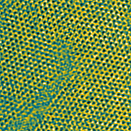
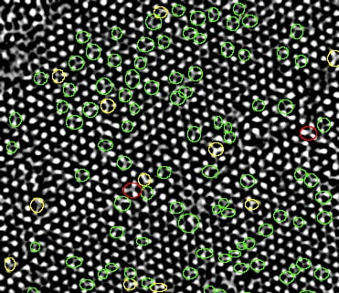
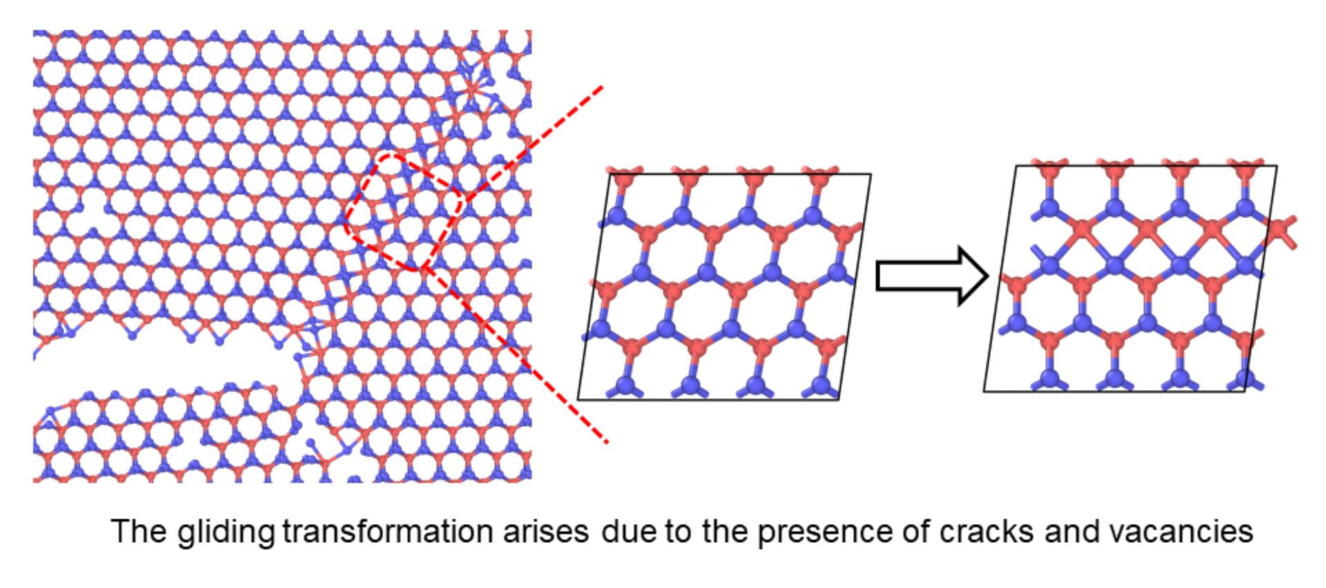
Currently, we are investigating TMDCs (specifically MoSe2 and MoTe2) owing to their versatility in electronic applications. In particular, their 2H phase is primarily used as semiconductors because of a bandgap(s) in the phonon dispersion band. Yet, TMDCs can transform to different phases due to the existence of defects. For example, we have discovered that multiple 0D and 1D chalcogenide vacancies will arise in MoSe2 monolayers by exposing them to electron irradiation with controlled dose rate. These defects can trigger distinctive grain boundaries with different structural features. The presence of these domains and boundaries can modify the monolayer’s electrical conductivity due to their metallic nature, opening an opportunity to engineer their pattern to acquire a desired conductivity. Additionally, these grain boundaries can also enhance the failure resistance of the material’s monolayer based on a mechanism similar to gliding in crystalline metals.
Defect engineering can also interfere at the synthesizing state. Along this path, the Micro and Nanomechanics Lab and our collaborators are investigating two types of defects: mirror twin boundaries observed in MoSe2 and the 1T-phase emergent in MoTe2. While the former has similar impact to chalcogenide vacancies, the latter brings unique features. By controlling the chemical potential of the synthesizing environment or manipulating the lattice of the substrate, a metallic phase of TMDCs, 1T, can arise. In this phase, instead of the ABA stacking seen in the 2H phase, the ABC stacking is dominating, which creates no band gap in its dispersion curve. The mixture of the two phases can be engineered to interfere with electrical and thermal conductivity.

SIZE SCALE AND RATE EFFECTS
Lorem Ipsum is simply dummy text of the printing and typesetting industry. Lorem Ipsum has been the industry’s standard dummy text ever since the 1500s, when an unknown printer took a galley of type and scrambled it to make point of using a type specimen book.
SELECT PUBLICATIONS
FRACTURE

In situ wear study reveals role of microstructure on self-sharpening mechanism in sea urchin teeth
H.D. Espinosa*†, A. Zaheri, H. Nguyen, D. Restrepo, M. Daly, M. Frank, J. McKittrick
Matter 1(5), 2019, pp. 1246-1261
The teeth of animals play a crucial role in their survival, and, like other body parts, they adapted to the host’s habitat to maximize their functionality. Superior performance in the sea urchin dentition system was hypothesized to emerge from sharpness preservation during the organism’s life span. In this work, a novel in situ scanning electron microscopy experimental methodology was employed to visualize a mechanism for sharpness preservation and to quantify conditions for its activation. Nonlinear finite-element modeling…
DEFECT ENGINEERING

Nanoscale toughening of ultrathin graphene oxide-polymer composites: mechano-chemical insights into hydrogen-bonding/van der Waals interactions, polymer chain alignment, and steric parameters
X. Zhang*, H. Nguyen*, M. Daly, S.B. T. Nguyen†, Horacio D Espinosa†
Nanoscale 11, 2019, pp. 12305-12316
This paper describes a systematic study on the nanoscale toughening of monolayer graphene oxide (GO) by an ultra-thin polymer adlayer, which impedes the propagation of cracks during intraplanar fracture. Using molecular dynamics simulations, the crack-bridging capabilities of a library of five hydrogen-bonding-capable polymers are explored against an epoxide-rich GO substrate. The best crack-bridging effect is found in polymers with functional groups…

Atomically thin polymer layer enhances toughness of graphene oxide monolayers
R.A. Soler-Crespo, L. Mao, J. Wen, H.T. Nguyen, X. Zhang, X. Wei, J. Huang†, S.B.T. Nguyen†, H.D. Espinosa†
Matter 1(2), 2019, pp. 369-388
Two-dimensional (2D) materials with unconventional properties have emerged as promising candidates for addressing societal needs for advanced electronic devices and strong lightweight composites. However, their intrinsic brittle behavior and the associated risk for catastrophic failure have thus far limited their adoption. Here, we demonstrate a strategy for extrinsically toughening these materials through engineering the surface chemistry of a graphene oxide ultrathin polymer model system…

The role of water in mediating interfacial adhesion and shear strength in graphene oxide
R.A. Soler-Crespo, W. Gao, L. Mao, H.T. Nguyen, M.R. Roenbeck, J.T. Paci, J. Huang†, S.B.T. Nguyen†, H.D. Espinosa†
ACS Nano 12(6), 2018, pp. 6089-6099
Graphene oxide (GO), whose highly tunable surface chemistry enables the formation of strong interfacial hydrogen-bond networks, has garnered increasing interest in the design of devices that operate in the presence of water. For instance, previous studies have suggested that controlling GO’s surface chemistry leads to enhancements in interfacial shear strength, allowing engineers to manage deformation pathways and control failure mechanisms. However, these previous…

Formulation and validation of a reduced order model of 2D materials exhibiting a two-phase microstructure as applied to graphene oxide
I. Benedetti*, H. Nguyen*, R.A. Soler-Crespo*, W. Gao, L. Mao, A. Ghasemi, J. Wen, S.B. Nguyen, H.D. Espinosa†
Journal of the Mechanics and Physics of Solids 112, 2018, pp. 66-88
Novel 2D materials, e.g., graphene oxide (GO), are attractive building blocks in the design of advanced materials due to their reactive chemistry, which can enhance interfacial interactions while providing good in-plane mechanical properties. Recent studies have hypothesized that the randomly distributed two-phase microstructure of GO, which arises due to its oxidized chemistry, leads to differences in nano- vs meso‑scale mechanical responses.

Engineering the mechanical properties of monolayer graphene oxide at the atomic level
R.A. Soler-Crespo*, W. Gao*, P. Xiao, X. Wei, J.T. Paci, G. Henkelman, H.D. Espinosa†
The Journal of Physical Chemistry Letters 7(14), 2016, pp. 2702-2707
The mechanical properties of graphene oxide (GO) are of great importance for applications in materials engineering. Previous mechanochemical studies of GO typically focused on the influence of the degree of oxidation on the mechanical behavior. In this study, using density functional-based tight binding simulations, validated using density functional theory simulations, we reveal that the deformation and failure of GO are strongly dependent on the relative concentrations of epoxide (−O−) and hydroxyl (−OH) functional groups.

Reliability of single crystal silver nanowire-based systems: stress assisted instabilities
R. Ramachandramoorthy*, Y. Wang*, A. Aghaei, G. Richter, W. Cai†, H.D. Espinosa†
ACS Nano 11(5), 2017, pp. 4768-4776
Time-dependent mechanical characterization of nanowires is critical to understand their long-term reliability in applications, such as flexible-electronics and touch screens. It is also of great importance to develop a theoretical framework for experimentation and analysis on the mechanics of nanowires under time-dependent loading conditions, such as stress-relaxation and fatigue. Here, we combine in situ scanning electron microscope (SEM)/transmission electron microscope (TEM) tests with atomistic and phase-field simulations to understand the deformation mechanisms of single crystal silver nanowires held under constant strain…
SIZE SCALE AND RATE EFFECTS
In Situ SEM High Strain Rate Testing of Large Diameter Micropillars Followed by TEM and EBSD Postmortem Analysis
Z. Lin, D.J. Magagnosc, J. Wen, C.-S. Oh, S.-M. Kim, H.D. Espinosa†
Experimental Mechanics 61, 2021, pp. 739-752
Dislocation dynamic simulations are intended as a tool to understand and predict the mechanical behavior of metallic materials, but its prediction has never been directly verified by experiments due to differences in specimen strain rate and size. In this work, a comprehensive experimental framework is proposed to attempt direct comparison between experiments and discrete dislocation dynamics (DDD) modelling. By integrating high-throughput sample fabrication and a customized testing apparatus, the sample size and strain rate typically employed in DDD simulations are explored experimentally.